US20260152687A1
COMPOSITION, METHOD OF TREATING METAL-CONTAINING LAYER, AND METHOD OF MANUFACTURING SEMICONDUCTOR DEVICE
Publication
Application
Classifications
IPC Classifications
CPC Classifications
Applicants
Samsung Electronics Co., Ltd.
Inventors
Jina KIM, Giho KO, Sungmin KIM, Youngchan KIM, Juhee MOON, Jinhye BAE, Wonsik YOON, Minhyung CHO, Cheol HAM, Kyuyoung HWANG
Abstract
Provided are a composition, a method of treating a metal-containing layer by using the composition, and a method of manufacturing a semiconductor device by using the composition. The composition may include an oxidizing agent, an ammonium-containing compound, and an etching controller. The etching controller may include a compound represented by Formula 1. A description of Formula 1 is provided herein.
Figures
Description
CROSS-REFERENCE TO RELATED APPLICATION
[0001]This application is based on and claims priority under 35 U.S.C. § 119 to Korean Patent Applications Nos. 10-2024-0177899, filed on Dec. 3, 2024, and 10-2025-0107689, filed on Aug. 5, 2025, in the Korean Intellectual Property Office, the disclosure of which is incorporated by reference herein in its entirety.
BACKGROUND
1. Field
[0002]The disclosure relates to a composition, a method of treating a metal-containing layer by using the composition, and/or a method of manufacturing a semiconductor device by using the composition.
2. Description of the Related Art
[0003]To meet the superior performance and low price demands of consumers, increased integration and improved reliability of electronic devices, for example semiconductor devices, may be required. As the integration of semiconductor devices increases, damage to the components of semiconductor devices during manufacturing processes of the semiconductor devices may have a greater impact on the reliability and/or electrical characteristics of semiconductor devices. In particular, during the manufacturing processes of semiconductor devices, various treatment processes, such as etching and cleaning processes, may be performed on a given layer (for example, a metal-containing layer). There may be a continuous demand for a composition having an appropriate etching rate and/or an excellent cleaning ability for performing an effective metal-containing layer treatment process.
SUMMARY
[0004]Provided are a composition having improved and/or excellent etching rate control performance, improved and/or excellent cleaning performance, and improved and/or excellent process stability, a method of treating a metal-containing layer using the composition, and/or a method of manufacturing a semiconductor device using the composition.
[0005]Additional aspects will be set forth in part in the description which follows and, in part, will be apparent from the description, or may be learned by practice of the presented embodiments of the disclosure.
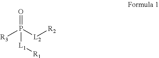
[0006]According to an example embodiment of the disclosure, a composition may include an oxidizing agent, an ammonium-containing compound, and an etching controller. The etching controller may include a compound represented by Formula 1.

- [0008]L1 and L2 may each independently be a single bond or oxygen,
- [0009]R1 may be hydrogen, a C1-C50 alkyl group, or a C2-C50 alkenyl group,
- [0010]R2 and R3 may each independently be a C1-C50 alkyl group or a C2-C50 alkenyl group, and
- [0011]in R2, R3, and R1 when R1 is not hydrogen, at least one hydrogen in each of the C1-C50 alkyl group and the C2-C50 alkenyl group may optionally be substituted with a halogen atom.
[0012]In some embodiments, the oxidizing agent may include hydrogen peroxide.
[0013]In some embodiments, the ammonium-containing compound may include dihydrogen phosphate ([H2PO4]−), hydrogen phosphate ([HPO4]2−), or phosphate ([PO4]3−).
[0014]In some embodiments, in Formula 1, i) L1 may be oxygen and L2 may be a single bond, or ii) L1 and L2 may each be oxygen.
[0015]In some embodiments, in Formula 1, R1 may be hydrogen or a C1-C5 alkyl group.
[0016]In some embodiments, in Formula 1, R2 and R3 may each independently be a branched C3-C50 alkyl group.
[0017]In some embodiments, the etching controller may further include an azole-containing compound and the azole-containing compound may include a pyrazole group, an imidazole group, a triazole group, or tetrazole group.
[0018]In some embodiments, a weight ratio of the compound represented by Formula 1 and the azole-containing compound may be selected from a range of 99:1 to 50:50.
- [0020]preparing a metal-containing layer including a first region and a second region, wherein a material in the first region of the metal-containing layer may be different from a material in the second region of the metal-containing layer; and
- [0021]contacting the metal-containing layer with a composition.
[0022]The first region of the metal-containing layer and the second region of the metal-containing layer may each independently include titanium (Ti), indium (In), aluminum (Al), lanthanum (La), scandium (Sc), gallium (Ga), copper (Cu), cobalt (Co), tungsten (W), ruthenium (Ru), molybdenum (Mo), zinc (Zn), hafnium (Hf), or any combination thereof.
[0023]The composition may include an oxidizing agent, an ammonium-containing compound, and an etching controller.
[0024]The etching controller comprises the compound represented by Formula 1.
[0025]In some embodiments, the first region of the metal-containing layer may include copper (Cu), cobalt (Co), tungsten (W), ruthenium (Ru), or any combination thereof.
[0026]In some embodiments, the second region of the metal-containing layer may include titanium nitride, titanium oxynitride, or any combination thereof.
[0027]In some embodiments, a second etching rate at which the composition etches the second region may be greater than a first etching rate at which the composition etches the first region.
- [0029]preparing a first insulating layer, a first conductive pattern in the first insulating layer, a second insulating layer on the first insulating layer, and an opening-forming mask pattern on the second insulating layer;
- [0030]forming an opening in the second insulating layer by etching the second insulating layer using the opening-forming mask pattern;
- [0031]contacting the opening-forming mask pattern and an exposed surface of the inside of the opening with a composition; and
- [0032]providing a conductive material in the opening, the conductive material being configured to be electrically connected to the first conductive pattern, wherein
- [0033]the composition may include an oxidizing agent, an ammonium-containing compound, and an etching controller, and
- [0034]the etching controller may include the compound represented by Formula 1.
[0035]In some embodiments, the first conductive pattern may include copper (Cu), cobalt (Co), tungsten (W), ruthenium (Ru), or any combination thereof.
[0036]In some embodiments, the opening-forming mask pattern may include titanium (Ti), indium (In), aluminum (Al), lanthanum (La), scandium (Sc), gallium (Ga), or any combination thereof.
[0037]In some embodiments, the opening-forming mask pattern may include a metal nitride, a metal oxynitride, or any combination thereof.
[0038]In some embodiments, the opening-forming mask pattern may include titanium nitride, titanium oxynitride, or any combination thereof. Each of the titanium nitride and the titanium oxynitride optionally further comprises indium (In), aluminum (Al), lanthanum (La), scandium (Sc), gallium (Ga), silicon (Si), or any combination thereof.
[0039]In some embodiments, the first conductive pattern may include a first barrier layer pattern and a first filling layer on the first barrier layer pattern.
[0040]In some embodiments, in the forming of the opening, a surface residue may be formed on at least one of a surface of the opening-forming mask pattern and the exposed surface of the inside of the opening, and the opening-forming mask pattern and the surface residue may be removed by the contacting the opening-forming mask pattern and the exposed surface of the inside of the opening with the composition.
BRIEF DESCRIPTION OF THE DRAWINGS
[0041]The above and other aspects, features, and advantages of certain embodiments of the disclosure will be more apparent from the following description taken in conjunction with the accompanying drawings, in which:
[0042]
[0043]
[0044]
[0045]
[0046]
[0047]
[0048]
[0049]
DETAILED DESCRIPTION
[0050]Reference will now be made in detail to embodiments, examples of which are illustrated in the accompanying drawings, wherein like reference numerals refer to like elements throughout. In this regard, the present embodiments may have different forms and should not be construed as being limited to the descriptions set forth herein. Accordingly, the embodiments are merely described below, by referring to the figures, to explain aspects. As used herein, the singular forms “a,” “an” and “the” are intended to include the plural forms as well, unless the context clearly indicates otherwise.
[0051]As used herein, the term “and/or” includes any and all combinations of one or more of the associated listed items. Expressions such as “at least one of,” when preceding a list of elements, modify the entire list of elements and do not modify the individual elements of the list. For example, “at least one of A, B, and C,” and similar language (e.g., “at least one selected from the group consisting of A, B, and C” and “at least one of A, B, or C”) may be construed as A only, B only, C only, or any combination of two or more of A, B, and C, such as, for instance, ABC, AB, BC, and AC.
[0052]When the terms “about” or “substantially” are used in this specification in connection with a numerical value, it is intended that the associated numerical value includes a manufacturing or operational tolerance (e.g., ±10%) around the stated numerical value. Moreover, when the words “generally” and “substantially” are used in connection with geometric shapes, it is intended that precision of the geometric shape is not required but that latitude for the shape is within the scope of the disclosure. Further, regardless of whether numerical values or shapes are modified as “about” or “substantially,” it will be understood that these values and shapes should be construed as including a manufacturing or operational tolerance (e.g., ±10%) around the stated numerical values or shapes. When ranges are specified, the range includes all values therebetween such as increments of 0.1%.
[0053]While the term “equal to” is used in the description of example embodiments, it should be understood that some imprecisions may exist. Thus, when one element is referred to as “equal to” another element, it should be understood that an element or a value may be “equal to” another element within a desired manufacturing or operational tolerance range (e.g., ±10%).
Metal-Containing Layer
[0054]A metal included in the metal-containing layer may include an alkali metal (for example, sodium (Na), potassium (K), rubidium (Rb), cesium (Cs), etc.), an alkaline earth metal (for example, beryllium (Be), magnesium (Mg), calcium (Ca), strontium (Sr), barium (Ba), etc.), a lanthanide metal (for example, lanthanum (La), europium (Eu), terbium (Tb), ytterbium (Yb), etc.), a transition metal (for example, scandium (Sc), yttrium (Y), titanium (Ti), zirconium (Zr), hafnium (Hf), vanadium (V), niobium (Nb), tantalum (Ta), chromium (Cr), molybdenum (Mo), tungsten (W), manganese (Mn), iron (Fe), ruthenium (Ru), osmium (Os), cobalt (Co), rhodium (Rh), nickel (Ni), copper (Cu), silver (Ag), zinc (Zn), etc.), a post-transition metal (for example, aluminum (AI), gallium (Ga), indium (In), thallium (TI), tin (Sn), or bismuth (Bi), etc.), or any combination thereof.
[0055]According to an embodiment, the metal included in the metal-containing layer may include Ti, In, Al, La, Sc, Ga, Cu, Co, W, Ru, Mo, Zn, Hf, or any combination thereof.
[0056]According to another embodiment, the metal-containing layer may include two or more different metals.
[0057]According to another embodiment, the metal-containing layer may include metal, a metal nitride, a metal oxide, a metal oxynitride, or any combination thereof.
[0058]According to another embodiment, the metal-containing layer may include titanium.
[0059]According to another embodiment, the metal-containing layer includes i) titanium (Ti), and may optionally further include ii) indium (In), aluminum (Al), lanthanum (La), scandium (Sc), gallium (Ga), tungsten (W), molybdenum (Mo), ruthenium (Ru), zinc (Zn), hafnium (Hf), silicon (Si), or any combination thereof, in addition to titanium (Ti). For example, the metal-containing layer may include titanium nitride, titanium nitride further including aluminum (e.g., TiAlN), titanium nitride further including lanthanum, titanium nitride further including silicon (e.g., TiSiN), or the like.
[0060]According to another embodiment, the metal-containing layer may include a conductive metal (e.g., copper, cobalt, tungsten, ruthenium, and the like).
[0061]According to another embodiment, the metal-containing layer may include i) a metal nitride, a metal oxynitride, or any combination thereof (e.g., titanium nitride, titanium oxynitride, or any combination thereof) and ii) a conductive metal (e.g., copper, cobalt, tungsten, ruthenium, and the like).
[0062]The metal-containing layer may be a single-layered structure including one or more materials, or a multi-layered structure including different materials. The plurality of layers included in the multi-layered structure may be vertically stacked or horizontally arranged with respect to the substrate. The single-layered structure and multi-layered structure may have various three-dimensional patterns (for example, via holes, trenches, etc.).
[0063]Meanwhile, the metal-containing layer may include a first region and a second region, and the first region and the second region may each independently include titanium (Ti), indium (In), aluminum (Al), lanthanum (La), scandium (Sc), gallium (Ga), copper (Cu), cobalt (Co), tungsten (W), ruthenium (Ru), molybdenum (Mo), zinc (Zn), hafnium (Hf), or any combination thereof, wherein a material included in the first region may be different from a material included in the second region.
[0064]According to an embodiment, the first region may include copper (Cu), cobalt (Co), tungsten (W), ruthenium (Ru), or any combination thereof.
[0065]According to another embodiment, the second region may include titanium (Ti), indium (In), aluminum (Al), lanthanum (La), scandium (Sc), gallium (Ga), or any combination thereof.
[0066]According to another embodiment, the first region may include a conductive metal (e.g., copper, cobalt, tungsten, and ruthenium).
[0067]According to another embodiment, the second region may include a metal nitride, a metal oxynitride, or any combination thereof (e.g., titanium nitride, titanium oxynitride, or any combination thereof).
[0068]According to another embodiment, the second region may include titanium nitride, titanium oxynitride, or any combination thereof. Each of the titanium nitride and titanium oxynitride may optionally further include indium (In), aluminum (Al), lanthanum (La), scandium (Sc), gallium (Ga), silicon (Si), or any combination thereof.
[0069]According to another embodiment, the second region may include i) titanium nitride, ii) titanium oxynitride, iii) titanium nitride further including indium (In), aluminum (Al), lanthanum (La), scandium (Sc), gallium (Ga), silicon (Si), or any combination thereof, iv) titanium oxynitride further including indium (In), aluminum (Al), lanthanum (La), scandium (Sc), gallium (Ga), silicon (Si), or any combination thereof, or v) any combination thereof.
Composition
[0070]The composition may include an oxidizing agent, an ammonium-containing compound, and an etching controller.
[0071]The composition may be used in various treatment processes for the metal-containing layer described herein, such as etching, cleaning, and polishing processes.
[0072]The composition may further include water (e.g., deionized water).
[0073]According to an embodiment, the composition may not include a polishing agent.
[0074]According to another embodiment, the composition may not include fluorine (F).
[0075]According to another embodiment, the composition may further include a pH regulator. For example, the pH regulator may be ammonium hydroxide, tetramethylammonium hydroxide (TMAH), or the like, but is not limited thereto.
[0076]Throughout the specification, the expression “etching a layer” may refer to removing at least a portion of a material constituting the layer.
Oxidizing Agent
[0077]The oxidizing agent serves to etch at least a portion of the metal-containing layer by oxidizing at least a portion of the metal (e.g., titanium) in the metal-containing layer to form a water-soluble complex, and may include, for example, at least one of hydrogen peroxide, nitric acid, and ammonium sulfate.
[0078]According to an embodiment, the oxidizing agent may include hydrogen peroxide.
[0079]According to another embodiment, the oxidizing agent may be hydrogen peroxide.
[0080]An amount (weight) of the oxidizing agent may be, for example, with respect to 100 wt % of the composition, about 1 wt % to about 50 wt %, about 10 wt % to about 50 wt %, about 16 wt % to about 50 wt %, about 18 wt % to about 50 wt %, about 20 wt % to about 50 wt %, about 22 wt % to about 50 wt %, about 25 wt % to about 50 wt %, about 1 wt % to about 45 wt %, about 10 wt % to about 45 wt %, about 16 wt % to about 45 wt %, about 18 wt % to about 45 wt %, about 20 wt % to about 45 wt %, about 22 wt % to about 45 wt %, about 25 wt % to about 45 wt %, about 1 wt % to about 40 wt %, about 10 wt % to about 40 wt %, about 16 wt % to about 40 wt %, about 18 wt % to about 40 wt %, about 20 wt % to about 40 wt %, about 22 wt % to about 40 wt %, about 25 wt % to about 40 wt %, about 1 wt % to about 35 wt %, about 10 wt % to about 35 wt %, about 16 wt % to about 35 wt %, about 18 wt % to about 35 wt %, about 20 wt % to about 35 wt %, about 22 wt % to about 35 wt %, about 25 wt % to about 35 wt %, about 1 wt % to about 30 wt %, about 10 wt % to about 30 wt %, about 16 wt % to about 30 wt %, about 18 wt % to about 30 wt %, about 20 wt % to about 30 wt %, about 22 wt % to about 30 wt %, about 25 wt % to about 30 wt %, about 16 wt % to about 27 wt %, about 18 wt % to about 27 wt %, about 20 wt % to about 27 wt %, about 22 wt % to about 27 wt %, or about 25 wt % to about 27 wt %.
[0081]When the amount of the oxidizing agent is within these ranges, the composition may have both improved and/or excellent etching selectivity and improved and/or excellent cleaning performance.
Ammonium-Containing Compound
[0082]The ammonium-containing compound may serve to maintain a high concentration of anions generated from the oxidizing agent and to stabilize a water-soluble complex generated when the anions oxidize at least a portion of the metal (e.g., titanium) in the metal-containing layer. By using such an ammonium-containing compound, at least a portion of the metal-containing layer may be more effectively etched.
[0083]The ammonium-containing compound may include an ammonium group.
[0084]According to an embodiment, the ammonium-containing compound may include an ammonium group represented by N(A11)(A12)(A13)(A14), wherein A11 to A14 may each independently be hydrogen, a C1-C30 alkyl group, a C2-C30 alkenyl group, a C3-C30 carbocyclic group, or a C1-C30 heterocyclic group.
[0085]For example, A11 to A14 may each independently be hydrogen or a C1-C10 alkyl group.
[0086]According to another embodiment, the ammonium-containing compound may not include fluorine (F). Without being limited by any particular theory, when the ammonium-containing compound does not include fluorine, accelerated corrosion of the surface of the metal-containing layer may be substantially limited and/or prevented, and the metal-containing layer treatment process using the composition may be performed in a safe and environmentally friendly atmosphere.
[0087]According to another embodiment, the ammonium-containing compound may include hydroxide, acetate, bicarbonate, benzoate, carbonate, formate, nitrate, hydrogen sulfate, carbamate, sulfamate, citrate, phosphate, sulfite, sulfobenzoate, oxalate, lactate, tartrate, dihydrogen citrate, glutamate, salicylate, bioxalate, octanoate, propionate, glycolate, or gluconate.
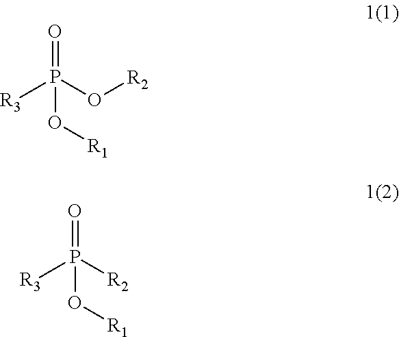
[0088]According to another embodiment, the ammonium-containing compound may include phosphate or hydroxide.
[0089]According to another embodiment, the ammonium-containing compound may include dihydrogen phosphate ([H2PO4]−), hydrogen phosphate ([HPO4]2−), or phosphate ([PO4]3−).
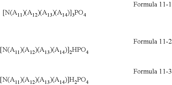
[0090]According to another embodiment, the ammonium-containing compound may include a compound represented by Formula 11-1, a compound represented by Formula 11-2, a compound represented by Formula 11-3, or any combination thereof:
[0091]wherein, in Formulae 11-1 to 11-3, A11 to A14 may each be the same as described herein.
[0092]According to another embodiment, the ammonium-containing compound may include at least one of ammonium phosphate ((NH4)3PO4), diammonium monohydrogen phosphate ((NH4)2HPO4), ammonium dihydrogen phosphate ((NH4)H2PO4), [N(CH3)4]3PO4, bis(tetramethylammonium) monohydrogen phosphate ([N(CH3)4]2HPO4), and tetramethylammonium dihydrogen phosphate ([N(CH3)4]H2PO4).
[0093]An amount (weight) of the ammonium-containing compound may be, for example, with respect to 100 wt % of the composition, about 0.01 wt % to about 10 wt %, about 0.05 wt % to about 10 wt %, about 0.1 wt % to about 10 wt %, about 0.3 wt % to about 10 wt %, about 0.5 wt % to about 10 wt %, about 0.01 wt % to about 7 wt %, about 0.05 wt % to about 7 wt %, about 0.1 wt % to about 7 wt %, about 0.3 wt % to about 7 wt %, about 0.5 wt % to about 7 wt %, about 0.01 wt % to about 4 wt %, about 0.05 wt % to about 4 wt %, about 0.1 wt % to about 4 wt %, about 0.3 wt % to about 4 wt %, about 0.5 wt % to about 4 wt %, about 0.01 wt % to about 2 wt %, about 0.05 wt % to about 2 wt %, about 0.1 wt % to about 2 wt %, about 0.3 wt % to about 2 wt %, about 0.5 wt % to about 2 wt %, about 0.01 wt % to about 1 wt %, about 0.05 wt % to about 1 wt %, about 0.1 wt % to about 1 wt %, about 0.3 wt % to about 1 wt %, about 0.5 wt % to about 1 wt %, about 0.01 wt % to about 0.7 wt %, about 0.05 wt % to about 0.7 wt %, about 0.1 wt % to about 0.7 wt %, about 0.3 wt % to about 0.7 wt %, about 0.5 wt % to about 0.7 wt %, about 0.01 wt % to about 0.5 wt %, about 0.05 wt % to about 0.5 wt %, about 0.1 wt % to about 0.5 wt %, or about 0.3 wt % to about 0.5 wt %.
[0094]When the amount of the ammonium-containing compound is within these ranges, the composition may have both improved and/or excellent etching selectivity and improved and/or excellent cleaning performance.
Etching Controller
[0095]The etching controller may serve to control the etching rate (e.g., suppress etching) and the like by interacting with various metal (e.g., copper, cobalt, tungsten, ruthenium, and the like) atoms in the metal-containing layer, which is a layer to be treated. In addition, the etching controller may serve to remove various surface residues generated during a deposition process and/or a patterning process of the metal-containing layer.
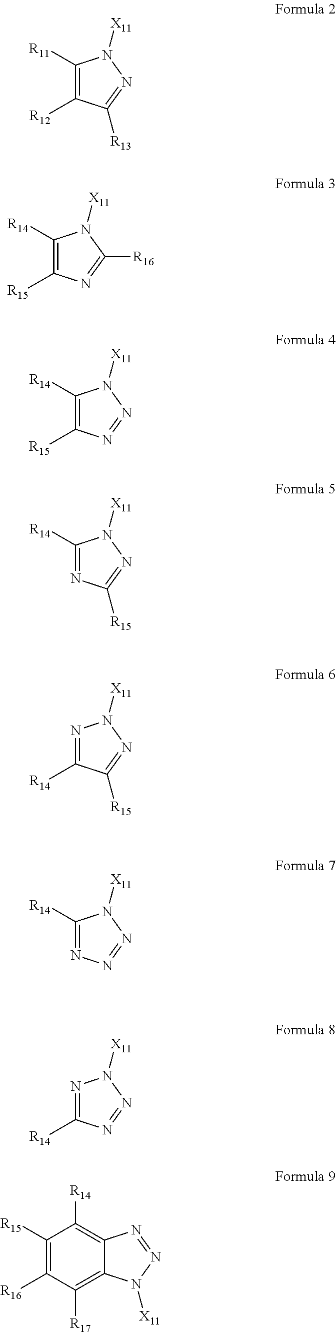
[0096]The etching controller may include a compound represented by Formula 1:
- [0097]wherein, in Formula 1,
- [0098]L1 and L2 may each independently be a single bond or oxygen,
- [0099]R1 may be hydrogen, a C1-C50 alkyl group, or a C2-C50 alkenyl group,
- [0100]R2 and R3 may each independently be a C1-C50 alkyl group or a C2-C50 alkenyl group, and
- [0101]in R2, R3, and R1 when R1 is not hydrogen, at least one hydrogen in each of the C1-C50 alkyl group and the C2-C50 alkenyl group may optionally be substituted with a halogen atom.
[0102]Each of the C1-C50 alkyl group and the C2-C50 alkenyl group may be linear or branched.
[0103]According to an embodiment, at least one of L1 and L2 of Formula 1 may be oxygen. Accordingly, the compound represented by Formula 1 and various metal (e.g., copper, cobalt, tungsten, ruthenium, and the like) atoms in the metal-containing layer may be effectively coordinated and bonded to each other, so that a protective layer including the compound represented by Formula 1 may be appropriately formed on the surface of the metal-containing layer. For example, in Formula 1, i) L1 may be oxygen and L2 may be a single bond, or ii) L1 and L2 may each be oxygen.
[0104]According to another embodiment, in Formula 1, R1 may be hydrogen or a C1-C20 alkyl group. For example, in Formula 1, R1 may be hydrogen or a C1-C10 alkyl group. As another example, in Formula 1, R1 may be hydrogen or a C1-C5 alkyl group (for example, methyl, etc.).
[0105]According to another embodiment, in Formula 1, R2 and R3 may each independently be a C1-C20 alkyl group or a C2-C20 alkenyl group. For example, in Formula 1, R2 and R3 may each independently be a C5-C20 alkyl group or a C5-C20 alkenyl group.
[0106]According to another embodiment, in Formula 1, R2 and R3 may each be a C5-C20 alkyl group, a C5-C10 alkyl group, a C6-C9 alkyl group, or a C7-C8 alkyl group.
[0107]According to another embodiment, in Formula 1, at least one of R2 and R3 (for example, R2 and R3) may each independently be a branched C3-C50 alkyl group, a branched C3-C20 alkyl group, a branched C5-C20 alkyl group, a branched C5-C10 alkyl group, a branched C6-C9 alkyl group, or a branched C7-C8 alkyl group.
[0108]According to another embodiment, in Formula 1, R2 and R3 may be identical to each other.
[0109]According to another embodiment, in Formula 1, R2 and R3 may be different from each other.
[0110]According to another embodiment, the etching controller may include a compound represented by Formula 1(1), a compound represented by Formula 1(2), or any combination thereof:
- [0111]wherein, in Formulae 1(1) and 1(2), R1 to R3 may each be the same as described herein.
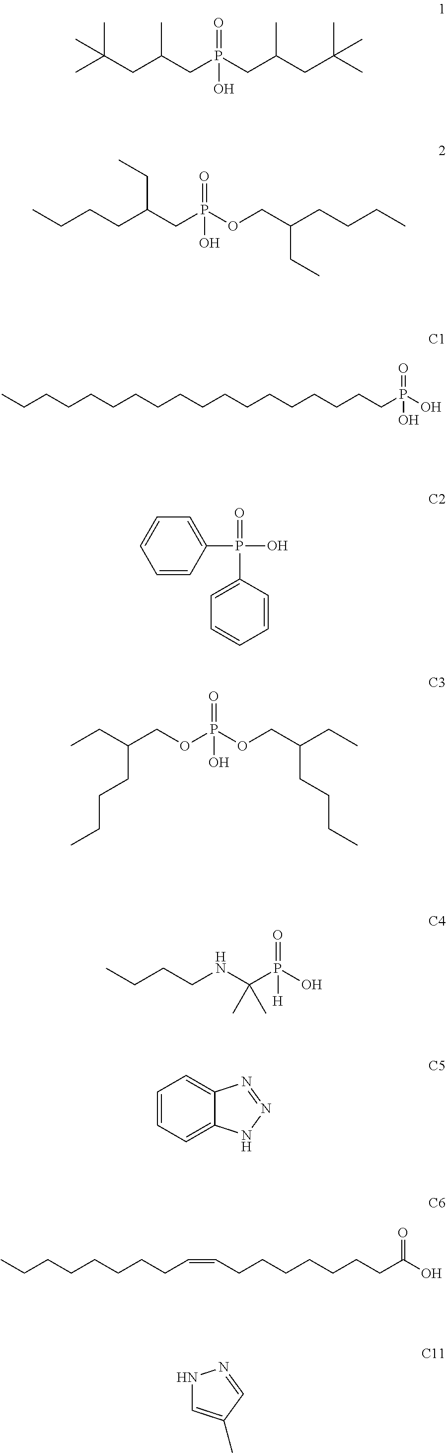
[0112]According to another embodiment, the etching controller may include at least one of Compounds 1 and 2:
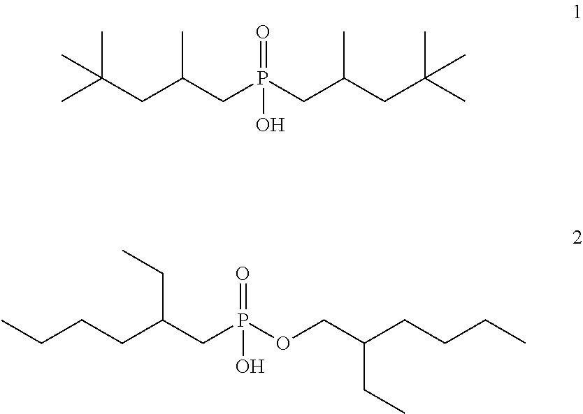
[0113]In Formula 1, R2 and R3 may each independently be a C1-C50 alkyl group or a C2-C50 alkenyl group. In addition, in Formula 1, hydrogens in each of the C1-C50 alkyl group and the C2-C50 alkenyl group, which may be R1 to R3, may be unsubstituted, or at least one hydrogen in each of the C1-C50 alkyl group and the C2-C50 alkenyl group, which may be R1 to R3, may be substituted with a halogen atom. Thus, for example, each of the C1-C50 alkyl group and the C2-C50 alkenyl group, which may be R1 to R3, may not include an alkoxy group, an alkylthio group, a phosphoric acid group, an amine derivative group, and the like as a substituent. Since a) R3 as defined above is a hydrophobic group and b) a group represented by *-L2-R2, wherein L2 is a single bond, is a hydrophobic group, a compound represented by Formula 1 may provide an appropriate hydrophobic protective layer to the surface of the metal-containing layer, which is a layer to be treated. In addition, by R2 and R3 as defined above, additional reactions between the hydrophobic protective layer and the metal ions surrounding it may be substantially limited and/or suppressed, so that the hydrophobic protective layer may be more easily removed together with various surface residues to be removed later. Therefore, during bringing the metal-containing layer into contact with the composition, control of selective etching rate (e.g., suppress of etching) with respect to certain metal may be effectively performed, and simultaneously, residues (the surface residue and/or an etching controller-derived residue) may not substantially remain on the surface of the metal-containing layer. Descriptions for the terms of the “surface residue” and the “etching controller-derived residue” may each be the same as described herein.
[0114]Furthermore, the compound represented by Formula 1 having R2 and R3 as defined above may have a large steric hindrance and may be difficult to be aligned regularly, so that micelles may not be substantially formed. Therefore, when manufacturing the composition and/or when treating a metal-containing layer using the composition, bubbles may not be substantially formed. Since the bubbles may cause a decrease in the efficiency and stability of the metal-containing layer treatment process, wafer damage, residue regeneration, contamination of various equipment, and the like, it may be advantageous to limit and/or prevent bubble formation when manufacturing the composition and/or when treating the metal-containing layer by using the composition. Without being limited by any particular theory, a composition with which bubble formation is observed during and/or immediately after the manufacture thereof may be substantially unsuitable for use in the treatment of the metal-containing layer, as the bubbles may interfere with uniform contact between the composition and the metal-containing layer and may be the cause of additional residue formation on the surface of the metal-containing layer.
[0115]Therefore, by using the composition including the compound represented by Formula 1, the etching rate may be selectively controlled depending on the metal in the metal-containing layer without bubble formation, and at the same time, the residues may be more effectively removed.
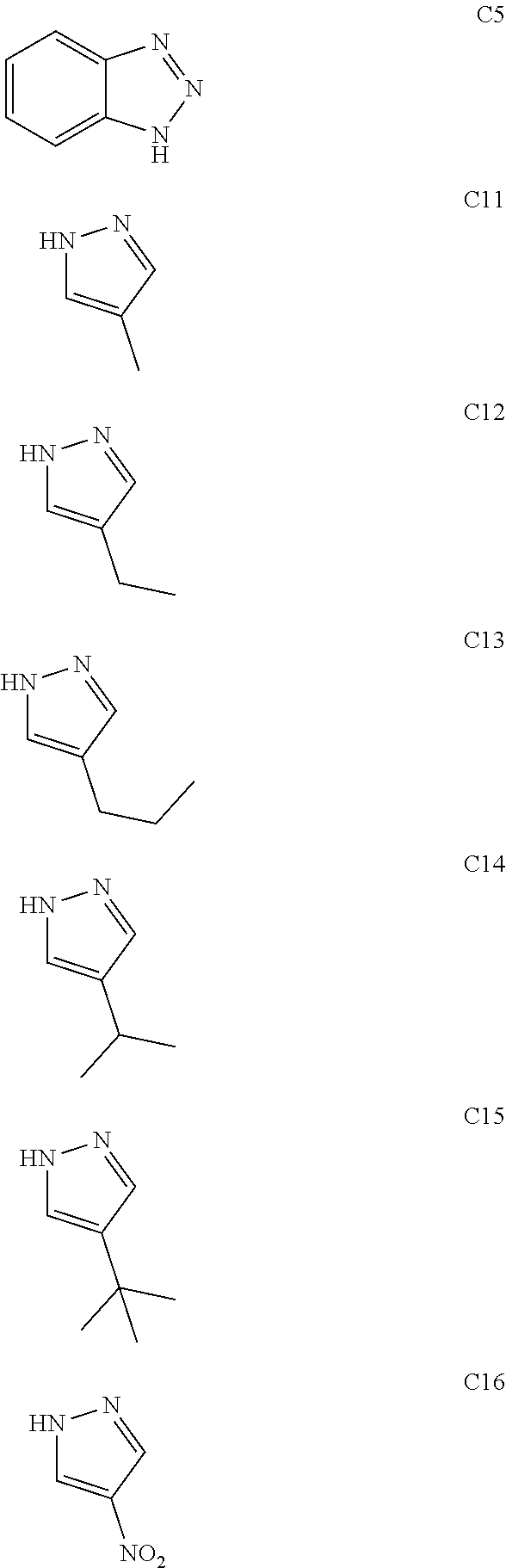
[0116]According to another embodiment, the etching controller may further include an azole-containing compound, in addition to the compound represented by Formula 1.
[0117]An azole in the azole-containing compound may include two, three, or four nitrogens as a ring-forming atom.
[0118]According to another embodiment, the azole-containing compound may include a pyrazole group, an imidazole group, a triazole group, or a tetrazole group.
[0119]According to another embodiment, the azole-containing compound may include a pyrazole group.
[0120]According to another embodiment, the azole-containing compound may include a compound represented by Formula 2, a compound represented by Formula 3, a compound represented by Formula 4, a compound represented by Formula 5, a compound represented by Formula 6, a compound represented by Formula 7, a compound represented by Formula 8, a compound represented by Formula 9, or any combination thereof:
- [0121]wherein, in Formulae 2 to 9,
- [0122]X11 may be hydrogen, a C1-C50 alkyl group, a C2-C50 alkenyl group, or a phenyl group,
- [0123]R11 to R17 may each independently be hydrogen, halogen, a nitro group (—NO2), a C1-C50 alkyl group, a C2-C50 alkenyl group, or a phenyl group, and
- [0124]in R11 to R17, and X11 when X11 is not hydrogen, at least one hydrogen in each of the C1-C50 alkyl group, the C2-C50 alkenyl group, and the phenyl group may optionally be substituted with a halogen atom.
[0125]According to another embodiment, X11 in Formulae 2 to 9 may be hydrogen.
[0126]According to another embodiment, R11 to R17 in Formulae 2 to 9 may each independently be hydrogen, halogen, a nitro group (—NO2), a C1-C10 alkyl group, a C2-C10 alkenyl group, or a phenyl group.
[0127]According to another embodiment, R11 to R17 in Formulae 2 to 9 may each independently be hydrogen, a nitro group (—NO2), or a C1-C4 alkyl group (for example, methyl, ethyl, propyl, isopropyl, n-butyl, sec-butyl, iso-butyl, tert-butyl, etc.).
[0128]According to another embodiment, at least one of R11, R12 and R13 in Formula 2 may each independently be halogen, a nitro group (—NO2), a C1-C50 alkyl group, a C2-C50 alkenyl group, or a phenyl group.
[0129]According to another embodiment, at least one of R11, R12 and R13 in Formula 2 may each independently be a nitro group (—NO2), a C1-C50 alkyl group, or a C2-C50 alkenyl group.
[0130]According to another embodiment, at least one of R11, R12 and R13 in Formula 2 may each independently be halogen, a nitro group (—NO2), a C1-C10 alkyl group, a C2-C10 alkenyl group, or a phenyl group.
[0131]According to another embodiment, at least one of R11, R12 and R13 in Formula 2 may each independently be a nitro group (—NO2), a C1-C10 alkyl group, or a C2-C10 alkenyl group.
[0132]According to another embodiment, at least one of R11, R12 and R13 in Formula 2 may each independently be a nitro group (—NO2), or a C1-C4 alkyl group (for example, methyl, ethyl, propyl, isopropyl, n-butyl, sec-butyl, iso-butyl, tert-butyl, etc.).
[0133]According to another embodiment, R12 in Formula 2 may be halogen, a nitro group (—NO2), a C1-C10 alkyl group, a C2-C10 alkenyl group, or a phenyl group.
[0134]According to another embodiment, R12 in Formula 2 may be a nitro group (—NO2), or a C1-C4 alkyl group.
[0135]According to another embodiment, R12 in Formula 2 may be a nitro group (—NO2), or a C1-C4 alkyl group and R11 and R13 in Formula 2 may each be hydrogen.
[0136]According to another embodiment, R14 to R17 in Formulae 3 to 9 may each be hydrogen.
[0137]According to another embodiment, the azole-containing compound may include the compound represented by Formula 2.
[0138]According to another embodiment, the azole-containing compound may include the compound represented by Formula 9.
[0139]According to another embodiment, the azole-containing compound may include at least one of Compound C5, C11, C12, C13, C14, C15 and C16:
[0140]According to another embodiment, a weight ratio of the compound represented by Formula 1 and the azole-containing compound may be selected from a range of 99:1 to 50:50, 95:5 to 50:50, or 90:10 to 50:50. For example, the weight ratio of the compound represented by Formula 1 and the azole-containing compound may be 65:35, 90:10, or 50:50.
[0141]According to another embodiment, an amount (weight) of the azole-containing compound may be, with respect to 100 wt % of a total amounts of the compound represented by Formula 1 and the azole-containing compound, about 5 wt % to about 60 wt %, about 10 wt % to about 60 wt %, about 5 wt % to about 50 wt %, or about 10 wt % to about 50 wt %.
[0142]By using the azole-containing compound in addition to the compound represented by Formula 1 in the composition, the etching rate may be more selectively controlled depending on the metal in the metal-containing layer and at the same time, the residues may be more effectively removed.
[0143]An amount (weight) of the etching controller may be, with respect to 100 wt % of the composition, about 0.001 wt % to about 10 wt %, about 0.01 wt % to about 10 wt %, about 0.1 wt % to about 10 wt %, about 0.15 wt % to about 10 wt %, about 0.2 wt % to about 10 wt %, about 0.001 wt % to about 5 wt %, about 0.01 wt % to about 5 wt %, about 0.1 wt % to about 5 wt %, about 0.15 wt % to about 5 wt %, about 0.2 wt % to about 5 wt %, about 0.001 wt % to about 1 wt %, about 0.01 wt % to about 1 wt %, about 0.1 wt % to about 1 wt %, about 0.15 wt % to about 1 wt %, about 0.2 wt % to about 1 wt %, about 0.001 wt % to about 0.5 wt %, about 0.01 wt % to about 0.5 wt %, about 0.1 wt % to about 0.5 wt %, about 0.15 wt % to about 0.5 wt %, about 0.2 wt % to about 0.5 wt %, about 0.001 wt % to about 0.3 wt %, about 0.01 wt % to about 0.3 wt %, about 0.1 wt % to about 0.3 wt %, about 0.15 wt % to about 0.3 wt %, or about 0.2 wt % to about 0.3 wt %.
[0144]The composition as described above may have a pH range of about 1.0 to about 10.0, about 3.0 to about 10.0, about 5.0 to about 10.0, about 7.0 to about 10.0, about 3.0 to about 8.0, about 5.0 to about 8.0, or about 7.0 to about 8.0. When the pH of the composition is within these ranges, the interaction between the etching controller and the metal atoms in the metal-containing layer as described below may occur more easily.
[0145]According to an embodiment, the composition may be used in a metal-containing layer treatment process, for example, an etching process, a cleaning process, and the like for a metal-containing layer. The description of the metal-containing layer may be as described herein.
[0146]Alternatively, the composition may also be used as an etching by-product remover, a post-etch process by-product remover, an ashing process by-product remover, a cleaning composition, a photoresist (PR) remover, an etching composition for a packaging process, a cleaning agent for a packaging process, a wafer adhesive remover, an etchant, a post-etch residue stripper, an ash residue cleaner, a PR residue stripper, or a post-CMP cleaner.
[0147]As used herein, the term “residue” refers to a material including at least one of the “surface residue” and the “etching controller-derived residue”.
[0148]As used herein, the term “surface residue” refers to by-products generated during deposition and/or patterning of the metal-containing layer. In the case where the surface residue remains on a metal-containing layer pattern formed after contact with the composition, the surface residue may cause an increase in electrical resistance and/or electrical short circuits between wirings. The surface residue may be an etching residue generated as a result of the etching process, and may include, for example, an etching gas-derived residue, an organic material-derived residue, a metal-containing residue or any combination thereof.
[0149]The etching gas-derived residue may be a residue derived from an etching gas used for dry etching. The etching gas may be, for example, fluorocarbon gas. For example, the etching gas may include CHF3, C2F6, CF4, C4F8, C2HF5, or the like. The etching gas-derived residue may include the etching gas itself and/or reaction product from reactions of the etching gas with materials in contact therewith during the etching process.
[0150]The organic material-derived residue may be an organic polymer or an organic-inorganic complex derived from various organic materials included in a photoresist, a dielectric layer, a buffer layer, a diffusion barrier layer, and the like used during manufacturing and/or patterning processes of the metal-containing layer. For example, the organic material-derived residue may be a polymer including carbon, silicon, fluorine, or any combination thereof.
[0151]The metal-containing residue may be any residue including a metal separated from the metal-containing layer during manufacturing and/or patterning processes of the metal-containing layer.
[0152]As used herein, the expression “etching controller-derived residue” refers to, for example, an aggregate including the etching controller, as a material insoluble in water due to high molecular weight thereof and remaining on the surface of the metal-containing layer even after rinsing and/or drying processes following the contact between the composition and the metal-containing layer. In the case where the etching controller-derived residue remains on the metal-containing layer pattern, the etching controller-derived residue may cause an increase in electrical resistance and/or electrical short circuits between wirings.
Method of Treating Metal-Containing Layer and Method of Manufacturing Electronic Device
[0153]A metal-containing layer including the first region and the second region, wherein the material included in the first region is different from the material included in the second region, may be more effectively treated by using the composition described above.
[0154]Therefore, a method of treating the metal-containing layer is provided, the method including preparing a substrate on which the metal-containing layer including the first region and the second region is provided, and bringing the metal-containing layer into contact with the composition. The metal-containing layer, the first region, and the second region are as described in the specification.
[0155]According to an embodiment, the first region and the second region may each independently include titanium (Ti), indium (In), aluminum (Al), lanthanum (La), scandium (Sc), gallium (Ga), copper (Cu), cobalt (Co), tungsten (W), ruthenium (Ru), molybdenum (Mo), zinc (Zn), hafnium (Hf), or any combination thereof.
[0156]According to an embodiment, the first region may include copper (Cu), cobalt (Co), tungsten (W), ruthenium (Ru), or any combination thereof.
[0157]According to another embodiment, the second region may include titanium (Ti), indium (In), aluminum (Al), lanthanum (La), scandium (Sc), gallium (Ga), or any combination thereof.
[0158]According to another embodiment, the first region may include a conductive metal (e.g., copper, cobalt, tungsten, ruthenium, or any combination thereof), and the second region may include a metal nitride, a metal oxynitride, or any combination thereof.
[0159]According to another embodiment, the second region may include titanium nitride, titanium oxynitride, or any combination thereof. Each of the titanium nitride and the titanium oxynitride may optionally further include indium (In), aluminum (Al), lanthanum (La), scandium (Sc), gallium (Ga), silicon (Si), or any combination thereof.
[0160]For example, the second region may include i) titanium nitride, ii) titanium oxynitride, iii) titanium nitride further including indium (In), aluminum (Al), lanthanum (La), scandium (Sc), gallium (Ga), silicon (Si), or any combination thereof, iv) titanium oxynitride further including indium (In), aluminum (Al), lanthanum (La), scandium (Sc), gallium (Ga), silicon (Si), or any combination thereof, or v) any combination thereof.
[0161]According to another embodiment, the first region may include copper (Cu), cobalt (Co), tungsten (W), ruthenium (Ru), or any combination thereof, and the second region may include titanium nitride, titanium oxynitride, or any combination thereof.
[0162]According to another embodiment, a second etching rate at which the composition etches the second region may be greater than a first etching rate at which the composition etches the first region. Thus, in the case where the first region and the second region of the metal-containing layer are brought into contact with the composition simultaneously, the second region may be etched faster than the first region. For example, by controlling a content ratio of compounds included in the composition, a contact time between the composition and the metal-containing layer, and the like, at least a portion of the second region or the entire second region may be etched without excessive etching (e.g., substantial etching) of the first region.
[0163]According to another embodiment, the second region of the metal-containing layer may be removed (for example, substantially removed) by the process of bringing the metal-containing layer into contact with the composition.
[0164]According to another embodiment, the surface residue is present on the metal-containing layer, and the second region of the metal-containing layer and the surface residue present thereon may be removed (for example, substantially removed) by the process of bringing the metal-containing layer into contact with the composition.
[0165]
[0166]As illustrated in
[0167]The substrate 10 may be a silicon substrate, a gallium arsenide substrate, a silicon germanium substrate, a ceramic substrate, a quartz substrate, a glass substrate for displays, a semiconductor substrate, or a semiconductor on insulator (SOI) substrate.
[0168]The metal-containing layer 20A of
[0169]For example, the first region 21 may include copper (Cu), cobalt (Co), tungsten (W), ruthenium (Ru), or any combination thereof, and the second region 22 may include titanium nitride, titanium oxynitride, or any combination thereof.
[0170]Surface residue R may be present on the surface of the metal-containing layer 20A of
[0171]The metal-containing layer 20A including the first region 21 and the second region 22 and provided with the surface residue R is brought into contact with the composition 30 as shown in
[0172]In the composition 30, i) the oxidizing agent may serve to etch at least a portion of the metal-containing layer 20A (for example, at least the second region 22) by oxidizing at least a portion of the metal in the metal-containing layer 20A to form a water-soluble complex, ii) the ammonium-containing compound may serve to maintain a high concentration of anions generated from the oxidizing agent and to effectively etch at least a portion of the metal-containing layer 20A (for example, at least the second region 22) by stabilizing the water-soluble complex generated when the anions oxidize at least a portion of the metal in the metal-containing layer 20A, and iii) the etching controller including the compound represented by Formula 1 having R2 and R3 as defined above may serve to selectively control the etching rate depending on the metal in the metal-containing layer 20A by selectively forming a hydrophobic protective layer without bubble formation, and at the same time, to more effectively remove the surface residue R generated during the deposition process and/or the patterning process of the metal-containing layer 20A. Therefore, the composition 30 as described above may be usefully used in various treatment processes for the metal-containing layer 20A.
[0173]According to another embodiment, upon contact with the composition 30, the surface of the first region 21 is substantially protected, and a second etching rate at which the composition 30 etches the second region 22 may be greater than a first etching rate at which the composition 30 etches the first region 21.
[0174]As a result, in the case where the first region 21 and the second region 22 of the metal-containing layer 20A are brought into contact with the composition 30 simultaneously, the second region 22 may be etched faster than the first region 21. For example, by controlling a content ratio of compounds included in the composition 30, a contact time between the composition 30 and the metal-containing layer 20A, and the like, at least a portion of the second region 22 may be etched as shown in
[0175]In addition, the composition 30 including the compound represented by Formula 1 as the etching controller may effectively remove both the surface residue R generated during the deposition process and/or the patterning process of the metal-containing layer 20A and the etching controller-derived residue, without bubble formation. Therefore, the residues (that is, the surface residue R in
[0176]Therefore, by using the composition including the oxidizing agent, the ammonium-containing compound, and the etching controller as described herein, both improved and/or excellent etching selectivity by controlling an etching rate for a certain metal and improved and/or excellent residue removal may be achieved “simultaneously”, and thus the metal-containing layer may be effectively treated at low cost.
[0177]Referring to
[0178]The electronic device may be, for example, various semiconductor devices.
[0179]Therefore, according to an embodiment, the preparing of a substrate on which is provided a metal-containing layer S100 and the contacting of the metal-containing layer with the composition S110 may be used in an opening (e.g., a trench, via hole pattern etc.) formation process for forming a bitline electrode in the method of manufacturing a semiconductor device.
[0180]Hereinafter, with reference to
[0181]
[0182]A second diffusion barrier layer 107 may be arranged on the first dielectric layer 103 and the metal layer 101 of
[0183]A second dielectric layer 109 may be arranged on the second diffusion barrier layer 107 of
[0184]On the second dielectric layer 109 of
[0185]A hard mask layer 113 may be arranged on the buffer layer 111 of
[0186]A first photoresist 115 may be arranged on the hard mask layer 113 of
[0187]Next, the first photoresist 115 may be patterned to form a first photoresist 115 pattern having a first opening having a width t as illustrated in
[0188]Next, as illustrated in
[0189]Thereafter, as illustrated in
[0190]Next, as illustrated in
[0191]As a result of the dry etching, a large amount of the surface residue R may exist on the inner wall of the trench and via hole pattern, as illustrated in
[0192]The surface residue R in
[0193]To this end, by contacting the composition including an oxidizing agent, an ammonium-containing compound, and an etching controller as described above with the substrate of
Method of Manufacturing Semiconductor Device
[0194]The composition may be effectively used in a method of manufacturing a semiconductor device.
[0195]Hereinafter, a method of manufacturing a semiconductor device using the composition according to an embodiment will be described with reference to
[0196]First, as shown in
[0197]The substrate 100 is as described with reference to the substrate 10 of
[0198]Insulating materials included in each of the first insulating layer 131 and the second insulating layer 132 may include various oxides, nitrides, oxynitrides, high dielectric materials, or any combination thereof. For example, the insulating material may include silicon oxide, silicon nitride, silicon oxynitride, aluminum oxide, hafnium oxide, hafnium oxynitride, zirconium oxide, or any combination thereof. The hafnium oxide and the hafnium oxynitride may optionally further include Si, Ta, Ti, Zr, or any combination thereof. As another example, the insulating material may include tetraethyl orthosilicate (TEOS), hydrogen silsesquioxane (HSQ), methyl silsesquioxane (MSQ), and the like. The first insulating layer 131 and the second insulating layer 132 may be formed as separate layers, as shown in
[0199]Although not illustrated in
[0200]For the material included in the first conductive pattern 121, see the material included in the first region of the metal-containing layer in the specification. For the material included in the opening-forming mask pattern 122, see the material included in the second region of the metal-containing layer in the specification. The first conductive pattern 121 may be, for example, wiring, via, or the like.
[0201]According to an embodiment, the first conductive pattern 121 may include copper (Cu), cobalt (Co), tungsten (W), ruthenium (Ru), or any combination thereof.
[0202]According to another embodiment, the opening-forming mask pattern 122 may include titanium (Ti), indium (In), aluminum (Al), lanthanum (La), scandium (Sc), gallium (Ga), or any combination thereof.
[0203]According to another embodiment, the opening-forming mask pattern 122 may include a metal nitride, a metal oxynitride, or any combination thereof.
[0204]According to another embodiment, the opening-forming mask pattern 122 may include titanium nitride, titanium oxynitride, or any combination thereof. Each of the titanium nitride and titanium oxynitride may optionally further include indium (In), aluminum (Al), lanthanum (La), scandium (Sc), gallium (Ga), silicon (Si), or any combination thereof. For example, the opening-forming mask pattern 122 may include i) titanium nitride, ii) titanium oxynitride, iii) titanium nitride further including indium (In), aluminum (Al), lanthanum (La), scandium (Sc), gallium (Ga), silicon (Si), or any combination thereof, iv) titanium oxynitride further including indium (In), aluminum (Al), lanthanum (La), scandium (Sc), gallium (Ga), silicon (Si), or any combination thereof, or v) any combination thereof.
[0205]According to another embodiment, the first conductive pattern 121 may include copper (Cu), cobalt (Co), tungsten (W), ruthenium (Ru), or any combination thereof, and the opening-forming mask pattern 122 may include titanium nitride, titanium oxynitride, or any combination thereof.
[0206]Subsequently, as shown in
[0207]Subsequently, as shown in
[0208]In the composition 30, i) the oxidizing agent may serve to etch and remove the opening-forming mask pattern 122 by oxidizing a metal (e.g., titanium) in the opening-forming mask pattern 122 to form a water-soluble complex, ii) the ammonium-containing compound may serve to maintain a high concentration of anions generated from the oxidizing agent and to effectively etch and remove the opening-forming mask pattern 122 by stabilizing the water-soluble complex generated when the anions oxidize a metal (e.g., titanium) in the opening-forming mask pattern 122, and iii) the etching controller including the compound represented by Formula 1 having R2 and R3 as defined above may serve to selectively control the etching rate by forming a hydrophobic protective layer on the first conductive pattern 121 to suppress excessive etching (e.g., substantial etching) of the first conductive pattern 121, without bubble formation, and at the same time, to effectively remove the surface residue R generated on the inside of the opening OP during the forming the opening OP.
[0209]For example, in the case where the opening-forming mask pattern 122 and the inside of the opening OP are brought into contact with the composition 30, the surface of the first conductive pattern 121 may be substantially protected, and thus a second etching rate at which the composition 30 etches the opening-forming mask pattern 122 may be greater than a first etching rate at which the composition 30 etches the first conductive pattern 121, thereby etching and removing the opening-forming mask pattern 122 without excessive etching (e.g., substantial etching) of the first conductive pattern 121 as shown in
[0210]In addition, the composition 30 including the compound represented by Formula 1 may effectively remove both the surface residue R and the etching controller-derived residue, without bubble formation. Therefore, the residues (that is, the surface residue R in
[0211]Therefore, by using the composition including the oxidizing agent, the ammonium-containing compound, and the etching controller as described herein, both selective etching for the opening-forming mask pattern 122 without substantially etching the surface of the first conductive pattern 121 and effective removal of the residues from the inside of the opening OP may be achieved “simultaneously”, and thus the opening OP may be effectively patterned at low cost.
[0212]Subsequently, a conductive material is introduced into the opening OP with being configured to be electrically connected to the first conductive pattern 141 to form a second conductive pattern 142 in contact with the second insulating layer 132 and electrically connected to the first conductive pattern 121 as shown in
[0213]The conductive material and the second conductive pattern 142 may include copper (Cu), carbon (C), silver (Ag), cobalt (Co), tantalum (Ta), indium (In), tin (Sn), zinc (Zn), manganese (Mn), titanium (Ti), magnesium (Mg), chromium (Cr), germanium (Ge), strontium (Sr), platinum (Pt), aluminum (Al), zirconium (Zr), tungsten (W), ruthenium (Ru), iridium (Ir), rhodium (Rh), or any combination thereof. Meanwhile, the conductive material and the second conductive pattern 142 may optionally further include titanium (Ti), titanium nitride (TiN), tantalum (Ta), tantalum nitride (TaN), tantalum carbonitride (TaCN), tungsten (W), tungsten nitride (WN), tungsten carbonitride (WCN), zirconium (Zr), zirconium nitride (ZrN), vanadium (V), vanadium nitride (VN), niobium (Nb), niobium nitride (NbN), or any combination thereof. The second conductive pattern 142 may be formed by using various methods such as atomic layer deposition (ALD) and chemical vapor deposition (CVD).
[0214]
[0215]
[0216]
[0217]
Examples 1 to 5 and Comparative Examples C1 to C6
[0218]25 wt % of hydrogen peroxide, 0.5 wt % of (NH4)2HPO4, etching controller, and tetramethylammonium hydroxide (TMAH) weighed in an amount selected within a range of 0.01 wt % to 0.5 wt % were mixed to prepare compositions of Examples 1 to 5 and Comparative Examples C1 to C6. As etching controllers in the compositions, the materials and the amounts listed in Table 1 were used. An amount of TMAH in each composition was selected to adjust the pH of each composition to 7.5, and the remainder of the composition corresponds to water (deionized water).
Comparative Example C7
[0219]A composition was prepared in the same manner as Example 1, except that the etching controller was not used.
Evaluation Example 1
[0220]After each of the compositions of Examples 1 to 5 and Comparative Examples C1 to C7 was manufactured, bubble formation was visually evaluated, and the results are summarized in Table 1.
| TABLE 1 | |||
|---|---|---|---|
| Ammonium- | |||
| Oxidizing | containing | Bubble |
| Classification | agent | compound | Etching controller | formation |
| Example 1 | Hydrogen | (NH4)2HPO4 | 1 | N |
| peroxide | (0.5 wt %) | (0.2 wt %) | ||
| (25 wt %) | ||||
| Example 2 | Hydrogen | (NH4)2HPO4 | 2 | N |
| peroxide | (0.5 wt %) | (0.2 wt %) | ||
| (25 wt %) | ||||
| Example 3 | Hydrogen | (NH4)2HPO4 | 1 | C11 | N |
| peroxide | (0.5 wt %) | (0.13 wt %) | (0.07 wt %) | ||
| (25 wt %) | |||||
| Example 4 | Hydrogen | (NH4)2HPO4 | 1 | C11 | N |
| peroxide | (0.5 wt %) | (0.18 wt %) | (0.02 wt %) | ||
| (25 wt %) | |||||
| Example 5 | Hydrogen | (NH4)2HPO4 | 1 | C5 | N |
| peroxide | (0.5 wt %) | (0.1 wt %) | (0.1 wt %) | ||
| (25 wt %) |
| Comparative | Hydrogen | (NH4)2HPO4 | C1 | Y |
| Example C1 | peroxide | (0.5 wt %) | (0.2 wt %) | |
| (25 wt %) | ||||
| Comparative | Hydrogen | (NH4)2HPO4 | C2 | N |
| Example C2 | peroxide | (0.5 wt %) | (0.2 wt %) | |
| (25 wt %) | ||||
| Comparative | Hydrogen | (NH4)2HPO4 | C3 | Y |
| Example C3 | peroxide | (0.5 wt %) | (0.2 wt %) | |
| (25 wt %) | ||||
| Comparative | Hydrogen | (NH4)2HPO4 | C4 | N |
| Example C4 | peroxide | (0.5 wt %) | (0.2 wt %) | |
| (25 wt %) | ||||
| Comparative | Hydrogen | (NH4)2HPO4 | C5 | N |
| Example C5 | peroxide | (0.5 wt %) | (0.2 wt %) | |
| (25 wt %) | ||||
| Comparative | Hydrogen | (NH4)2HPO4 | C6 | Y |
| Example C6 | peroxide | (0.5 wt %) | (0.2 wt %) | |
| (25 wt %) | ||||
| Comparative | Hydrogen | (NH4)2HPO4 | — | N |
| Example C7 | peroxide | (0.5 wt %) | ||
| (25 wt %) | ||||
| “N” for bubble formation: No bubbles observed. | ||||
| “Y” for bubble formation: Bubbles observed. | ||||
[0221]From
[0222]From
Evaluation Example 2
[0223]As shown in
[0224]Thereafter, the composition of Example 1 was placed in each of two beakers and heated to 50° C., and a copper film and a cobalt film, which were subjected to dipping in a mixture of HF and water with a volume ratio of 1:200 for 40 seconds at room temperature, were immersed in the respective beakers for 10 minutes and 5 minutes. Then, the thicknesses of the copper film and the cobalt film were measured by using X-ray fluorescence spectrometry (XRF) (S8 Tiger, BRUKER) to evaluate the rate at which the composition of Example 1 etches the copper film (Å/min), and the rate at which the composition of Example 1 etches the cobalt film (Å/min). The results are summarized in Table 2.
[0225]The tests were repeated using each of the compositions of Examples 2 to 5 and Comparative Examples C2, C4, C5, and C7, and the results are summarized in Table 2.
| TABLE 2 | |||
|---|---|---|---|
| Etching | Etching | ||
| Ammonium- | rate for | rate for |
| Oxidizing | containing | Etching | Residue | Cu film | Co film | ||
| Classification | agent | compound | controller | pH | removal | (Å/min) | (Å/min) |
| Example | Hydrogen | (NH4)2HPO4 | 1 | 7.5 | Good | 0.4 | 1.2 |
| 1 | peroxide | (0.5 wt %) | (0.2 wt %) |
| (25 wt %) |
| Example | Hydrogen | (NH4)2HPO4 | 2 | 7.5 | Good | 0.8 | 3.2 |
| 2 | peroxide | (0.5 wt %) | (0.2 wt %) |
| (25 wt %) | ||||||||
| Example | Hydrogen | (NH4)2HPO4 | 1 | C11 | 7.5 | Good | <0.1 | 0.2 |
| 3 | peroxide | (0.5 wt %) | (0.13 | (0.07 | ||||
| (25 wt %) | wt %) | wt %) | ||||||
| Example | Hydrogen | (NH4)2HPO4 | 1 | C11 | 7.5 | Good | <0.1 | 0.5 |
| 4 | peroxide | (0.5 wt %) | (0.18 | (0.02 | ||||
| (25 wt %) | wt %) | wt %) | ||||||
| Example | Hydrogen | (NH4)2HPO4 | 1 | C5 | 7.5 | Good | 1.6 | 0.1 |
| 5 | peroxide | (0.5 wt %) | (0.1 | (0.1 | ||||
| (25 wt %) | wt %) | wt %) |
| Comparative | Hydrogen | (NH4)2HPO4 | C2 | 7.5 | Poor | 0.9 | 11.4 |
| Example | peroxide | (0.5 wt %) | (0.2 wt %) |
| C2 | (25 wt %) |
| Comparative | Hydrogen | (NH4)2HPO4 | C4 | 7.5 | Poor | 0.2 | 11.1 |
| Example | peroxide | (0.5 wt %) | (0.2 wt %) |
| C4 | (25 wt %) |
| Comparative | Hydrogen | (NH4)2HPO4 | C5 | 7.5 | Poor | 2.6 | 0.2 |
| Example | peroxide | (0.5 wt %) | (0.2 wt %) |
| C5 | (25 wt %) |
| Comparative | Hydrogen | (NH4)2HPO4 | — | 7.5 | Poor | 1.4 | >10 |
| Example | peroxide | (0.5 wt %) | ||||||
| C7 | (25 wt %) | |||||||
| “Good” residue removal: No residue of 10 nm or more in length was observed. | ||||||||
| “Poor” residue removal: Residues of 10 nm or more in length were observed. | ||||||||
[0226]In
[0227]In addition, from Table 2, it can be confirmed that i) the compositions of Examples 1 to 4 had superior copper film etching inhibition performance compared to the compositions of Comparative Examples C2, C5, and C7, and ii) the compositions of Examples 1 to 5 had superior cobalt film etching inhibition performance compared to the compositions of Comparative Examples C2, C4, and C7.
[0228]From
[0229]The composition has improved and/or excellent etching rate control performance and improved and/or excellent cleaning performance without bubble formation, and thus, may be effectively used in various treatment processes for various metal-containing layers, such as etching and cleaning processes. Therefore, by treating a metal-containing layer using the composition, higher-quality electronic devices may be manufactured.
[0230]It should be understood that embodiments described herein should be considered in a descriptive sense only and not for purposes of limitation. Descriptions of features or aspects within each embodiment should typically be considered as available for other similar features or aspects in other embodiments. While one or more embodiments have been described with reference to the figures, it will be understood by those of ordinary skill in the art that various changes in form and details may be made therein without departing from the spirit and scope as defined by the following claims.
Claims
What is claimed is:
1. A method of manufacturing a semiconductor device, the method comprising:
preparing a first insulating layer, a first conductive pattern in the first insulating layer, a second insulating layer on the first insulating layer, and an opening-forming mask pattern on the second insulating layer;
forming an opening in the second insulating layer by etching the second insulating layer using the opening-forming mask pattern;
contacting the opening-forming mask pattern and an exposed surface of an inside of the opening with a composition; and
providing a conductive material in the opening, the conductive material being configured to be electrically connected to the first conductive pattern, wherein
the composition comprises an oxidizing agent, an ammonium-containing compound, and an etching controller, and
the etching controller comprises a compound represented by Formula 1,

wherein, in Formula 1,
L1 and L2 are each independently a single bond or oxygen,
R1 is hydrogen, a C1-C50 alkyl group, or a C2-C50 alkenyl group,
R2 and R3 are each independently a C1-C50 alkyl group or a C2-C50 alkenyl group, and
in R2, R3, and R1 when R1 is not hydrogen, at least one hydrogen in each of the C1-C50 alkyl group and the C2-C50 alkenyl group is optionally substituted with a halogen atom.
2. The method of
wherein the first conductive pattern comprises copper (Cu), cobalt (Co), tungsten (W), ruthenium (Ru), or any combination thereof, and
the opening-forming mask pattern comprises titanium (Ti), indium (In), aluminum (Al), lanthanum (La), scandium (Sc), gallium (Ga), or any combination thereof.
3. The method of
wherein the opening-forming mask pattern comprises a metal nitride, a metal oxynitride, or any combination thereof.
4. The method of
wherein the opening-forming mask pattern comprises titanium nitride, titanium oxynitride, or any combination thereof, and
each of the titanium nitride and the titanium oxynitride optionally further comprises indium (In), aluminum (Al), lanthanum (La), scandium (Sc), gallium (Ga), silicon (Si), or any combination thereof.
5. The method of
wherein the first conductive pattern comprises a first barrier layer pattern and a first filling layer on the first barrier layer pattern.
6. The method of
during the forming of the opening, a surface residue is formed on at least one of a surface of the opening-forming mask pattern and the exposed surface of the inside of the opening, and
the opening-forming mask pattern and the surface residue are removed by the contacting the opening-forming mask pattern and the exposed surface of the inside of the opening with the composition.
7. The method of
wherein the ammonium-containing compound of the composition comprises dihydrogen phosphate ([H2PO4]−), hydrogen phosphate ([HPO4]2−), or phosphate ([PO4]3−).
8. The method of
in Formula 1, R2 and R3 are each a branched C3-C50 alkyl group.
9. The method of
an amount of the etching controller is about 0.001 wt % to about 10 wt % with respect to 100 wt % of the composition.
10. A composition comprising:
an oxidizing agent;
an ammonium-containing compound; and
an etching controller, wherein
the etching controller comprises a compound represented by Formula 1:

wherein, in Formula 1,
L1 and L2 are each independently a single bond or oxygen,
R1 is hydrogen, a C1-C50 alkyl group, or a C2-C50 alkenyl group,
R2 and R3 are each independently a C1-C50 alkyl group or a C2-C50 alkenyl group, and
in R2, R3, and R1 when R1 is not hydrogen, at least one hydrogen in each of the C1-C50 alkyl group and the C2-C50 alkenyl group is optionally substituted with a halogen atom.
11. The composition of
12. The composition of
wherein the ammonium-containing compound of the composition comprises dihydrogen phosphate ([H2PO4]−), hydrogen phosphate ([HPO4]2−), or phosphate ([PO4]3−).
13. The composition of
the ammonium-containing compound comprises a compound represented by Formula 11-1, a compound represented by Formula 11-2, a compound represented by Formula 11-3, or any combination thereof,
wherein, in Formulae 11-1 to 11-3, A11 to A14 are each independently hydrogen, a C1-C30 alkyl group, a C2-C30 alkenyl group, a C3-C30 carbocyclic group, or a C1-C30 heterocyclic group.
14. The composition of
15. The composition of
in Formula 1, R2 and R3 are each a branched C3-C50 alkyl group.
16. The composition of
wherein the etching controller further comprises an azole-containing compound and the azole-containing compound comprises a pyrazole group, an imidazole group, a triazole group, or tetrazole group.
17. The composition of
an amount of the etching controller is about 0.001 wt % to about 10 wt % with respect to 100 wt % of the composition.
18. A method of treating a metal-containing layer, the method comprising:
preparing a metal-containing layer including a first region and a second region, wherein a material in the first region of the metal-containing layer is different from a material in the second region of the metal-containing layer; and
contacting the metal-containing layer with a composition,
wherein the first region of the metal-containing layer and the second region of the metal-containing layer each independently comprise titanium (Ti), indium (In), aluminum (Al), lanthanum (La), scandium (Sc), gallium (Ga), copper (Cu), cobalt (Co), tungsten (W), ruthenium (Ru), molybdenum (Mo), zinc (Zn), hafnium (Hf), or any combination thereof,
the composition comprises an oxidizing agent, an ammonium-containing compound, and an etching controller, and
the etching controller comprises a compound represented by Formula 1:

wherein, in Formula 1,
L1 and L2 are each independently a single bond or oxygen,
R1 is hydrogen, a C1-C50 alkyl group, or a C2-C50 alkenyl group,
R2 and R3 are each independently a C1-C50 alkyl group or a C2-C50 alkenyl group, and
in R2, R3, and R1 when R1 is not hydrogen, at least one hydrogen in each of the C1-C50 alkyl group and the C2-C50 alkenyl group is optionally substituted with a halogen atom.
19. The method of
the first region of the metal-containing layer comprises copper (Cu), cobalt (Co), tungsten (W), ruthenium (Ru), or any combination thereof, and
the second region of the metal-containing layer comprises titanium (Ti), indium (In), aluminum (Al), lanthanum (La), scandium (Sc), gallium (Ga), or any combination thereof.
20. The method of
a second etching rate at which the composition etches the second region of the metal-containing layer is greater than a first etching rate at which the composition etches the first region of the metal-containing layer.