US20250293202A1
RESIN COMPOSITION AND METHOD OF FORMING A SEMICONDUCTOR PACKAGE WITH UNDERFILL USING THE SAME
Publication
Application
Classifications
IPC Classifications
CPC Classifications
Applicants
Samsung Electronics Co., Ltd.
Inventors
Taehyung Lee, Joonhyeok Jang
Abstract
A method of manufacturing a semiconductor package that includes mounting a semiconductor chip on a substrate, dispensing a resin composition to a first side of the semiconductor chip, in which the resin composition includes a filling portion flowing to an inside region of the semiconductor chip between the semiconductor chip and the substrate, and an outside portion flowing outside the semiconductor chip; and projecting infrared light onto at least a portion of the outside portion of the resin composition, while the resin composition flows to an opposite side of the semiconductor chip that is opposite from the first side of the semiconductor, wherein the resin composition includes 20 to 40 10 wt % of an epoxy resin, 5 to 10 wt % of a curing agent, 50 to 70 wt % of a filler, and 1 to 5 wt % of an infrared absorber.
Figures
Description
CROSS-REFERENCE TO RELATED APPLICATIONS
[0001]This U.S. non-provisional application claims the benefit of priority under 35 U.S.C. § 119 to Korean Patent Application No. 10-2024-0036120 filed on Mar. 15, 2024, in the Korean Intellectual Property Office, the disclosure of which is incorporated herein by reference in its entirety.
BACKGROUND
[0002]The present inventive concept relates to a resin composition, a method of forming underfill using the same, and a method of manufacturing a semiconductor package using the same.
[0003]As the bump pitch of semiconductor chips has recently become smaller, there is a need for development to improve the fluidity and filling properties of underfill materials injected between a substrate and a semiconductor chip. If the viscosity of underfill materials is low, fluidity and filling properties may be improved, but underfill materials may flow to the outside of the semiconductor chip and cause various defects.
SUMMARY
[0004]An aspect of the present inventive concept is to provide a method of controlling flow of underfill and forming underfill with improved reliability.
[0005]According to an aspect of the present inventive concept, a method of forming underfill or manufacturing a semiconductor package includes: mounting a semiconductor chip on a substrate; dispensing a resin composition to a first side of the semiconductor chip in which the resin composition includes a filling portion flowing to an inside region of the semiconductor chip between the semiconductor chip between the semiconductor chip and the substrate, and an outside portion flowing outside of the semiconductor chip; and projecting infrared light onto at least a portion of the outside portion of the resin composition, while the resin composition flows to an opposite side of the semiconductor chip that is opposite from the first side of the semiconductor chip, in which the resin composition includes 20 to 40 wt % of an epoxy resin; 5 to 10 wt % of a curing agent; 50 to 70 wt % of a filler; and 1 to 5 wt % of an infrared absorber.
[0006]According to an aspect of the present inventive concept, a method of forming underfill or method of manufacturing a semiconductor package includes: mounting a semiconductor chip on a substrate; dispensing a resin composition including an infrared absorber to a first side of the semiconductor chip between the semiconductor chip and the substrate, and out outside portion flowing outside the semiconductor chip, in which the resin composition includes a filling portion flowing to an inside region of the semiconductor chip between the semiconductor chip and the substrate, and an outside portion flowing to a region outside of the semiconductor chip; and projecting infrared light onto at least a portion of the resin composition, while the resin composition flows between the semiconductor chip and the substrate from the first side of the semiconductor chip, in which the outside portion includes a first outside portion adjacent to a first side surface of the semiconductor chip corresponding to the first side of the semiconductor chip and a second outside portion adjacent to a second side surface of the semiconductor chip, intersecting the first side surface, in which the infrared light is projected onto the second outside portion, and in which a second width of the second outside portion is smaller than a first width of the first outside portion.
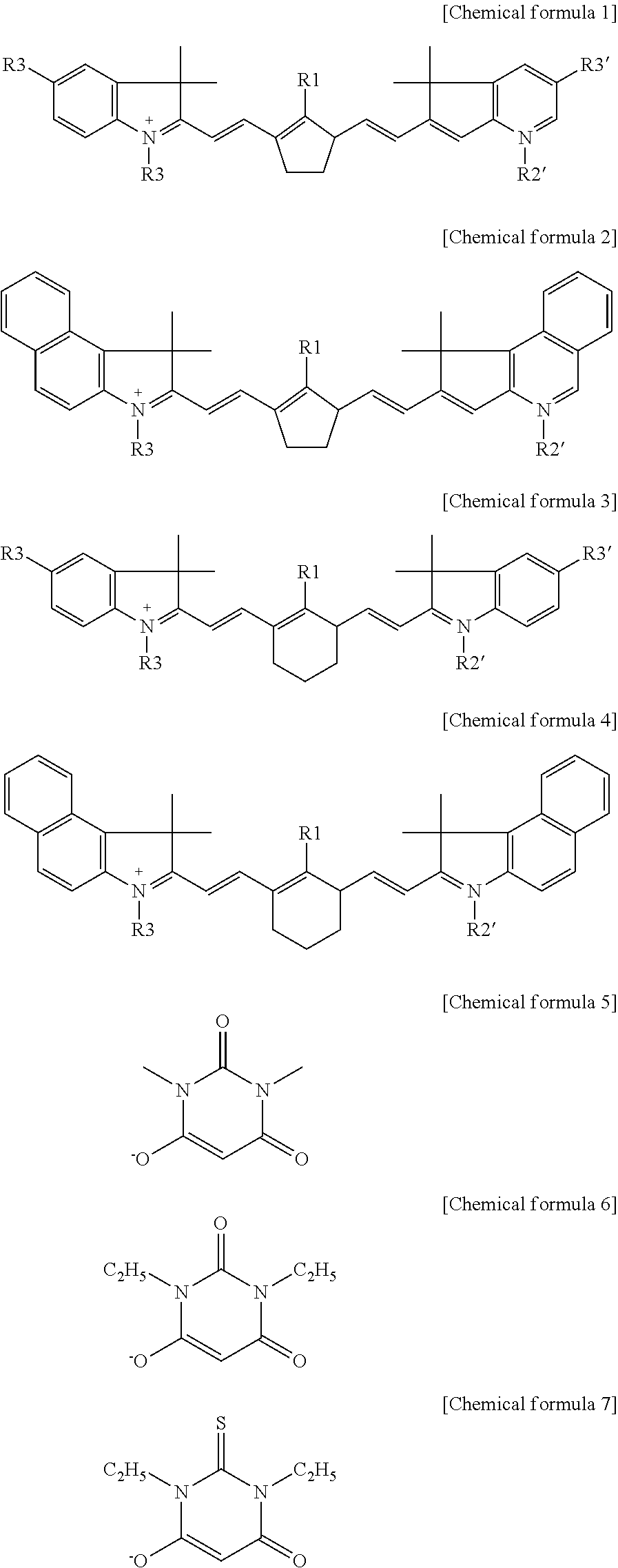
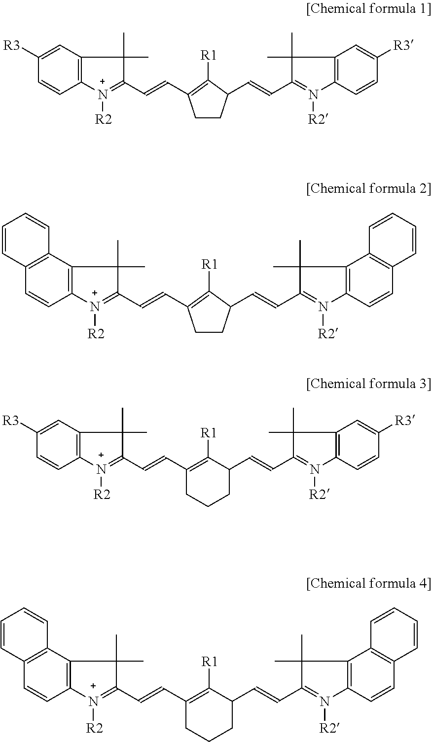
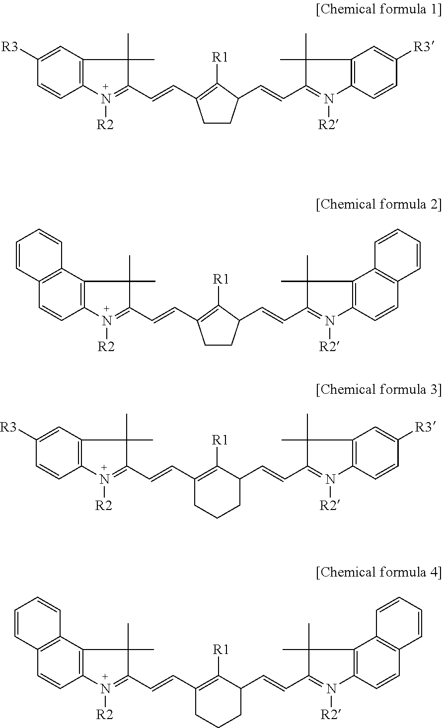
[0007]According to an aspect of the present inventive concept, a resin composition includes: 20 to 40 wt % of an epoxy resin; 5 to 10 wt % of a curing agent; 50 to 70 wt % of a filler; and 1 to 5 wt % of an infrared absorber including a compound having at least one structure selected from Chemical formula 1, Chemical formula 2, Chemical formula 3, and Chemical formula 4 below,
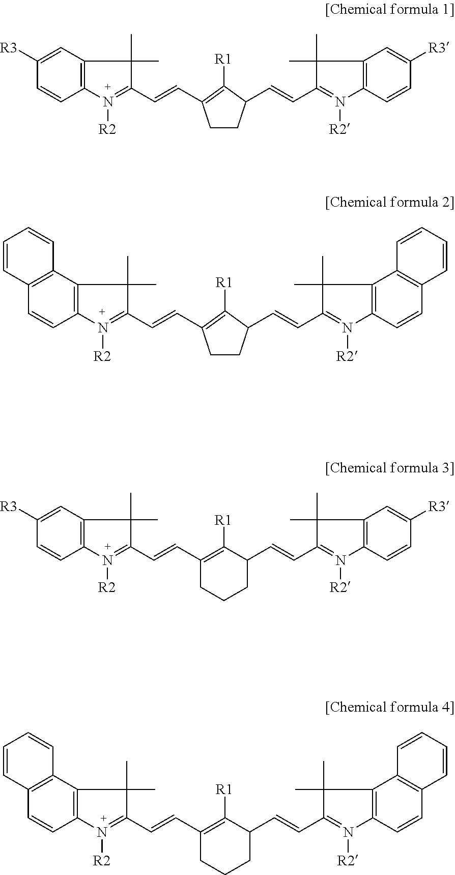
(wherein R1 includes a barbiturate group, R2 and R2′ include at least one group selected from a methyl group, an ethyl group, and a 3-methylbutyl group, and R3 and R3′ include hydrogen or chlorine).
BRIEF DESCRIPTION OF DRAWINGS
[0008]The above and other aspects, features, and advantages of the present inventive concept will be more clearly understood from the following detailed description, taken in conjunction with the accompanying drawings, in which:
[0009]
[0010]
[0011]
[0012]
[0013]
[0014]
[0015]
[0016]
DETAILED DESCRIPTION
[0017]Embodiments of the present inventive concept will be described herein with reference to the attached drawings.
[0018]Unless otherwise specified, in this specification, terms, such as ‘upper pad,’ ‘lower pad,’ ‘side surface,’ etc. are based on the drawings, and may vary in the directions in which components are actually arranged.
[0019]In addition, ordinal numbers, such as “first,” “second,” “third,” etc. may be used as labels for specific elements, steps, directions, etc. to distinguish various elements, steps, directions, etc. from each other, and are not meant to be limiting. Terms that are not described using “first,” “second,” etc. in the specification may still be referred to as “first” or “second” in the claims. In addition, terms referenced by a particular ordinal number (e.g., “first” in a particular claim) may be described elsewhere with a different ordinal number (e.g., “second” in the specification or other claims).
[0020]It will be understood that the terms “includes” and/or “including” when used in this specification, specify the presence of stated features, regions, integers, steps, operations, elements, and/or components, but do not preclude the presence or addition of one or more other features, regions, integers, steps, operations, elements, components, and/or groups thereof.
[0021]As used herein, the term “and/or” includes any and all combinations of one or more of the associated listed items and may be abbreviated as “/”. Items described in the singular herein may be provided in plural, as can be seen, for example, in the drawings. Thus, the description of a single item that is provided in plural should be understood to be applicable to the remaining plurality of items unless context indicates otherwise.
[0022]
[0023]Referring to
[0024]In example embodiments, the steps shown in
[0025]The underfill forming method (S100) of an example embodiment may use a resin composition configured to convert light in an infrared region into thermal energy.
[0026]The resin composition of an example embodiment may include an epoxy resin, a curing agent, a filler, and an infrared absorber. According to an embodiment, the resin composition may further include an additive. The resin composition described herein may be understood as being applied to the resin composition 103 shown in
[0027]The epoxy resin may include at least one epoxy component selected from the group consisting of a bisphenol-A epoxy, a bisphenol-F epoxy, rubber modified epoxy, novolac epoxy, cycloaliphatic epoxy, tetra-functional epoxy, acryl modified epoxy, coal tar modified epoxy, aliphatic chain modified epoxy, cresol novolac epoxy, polyglycol epoxy, cardanol epoxy, brominated epoxy, and phenoxy epoxy. The epoxy resin may be included in 20 wt % to 40 wt % of the total composition.
[0028]The curing agent may include at least one curing agent selected from the group consisting of an acid anhydride-based curing agent, a cationic curing agent, an imidazole curing agent, a dicyandiamide curing agent, and an amine adduct curing agent. The curing agent may be included in 5 wt % to 10 wt % of the total composition.
[0029]The acid anhydride-based curing agent may include at least one curing agent selected from the group consisting of dodecenyl succinic anhydride (DDSA), polyadipic acid (PADA), polysebacic acid (PSPA), methyl tetrahydrophthalic anhydride (Me-THPA), methyl hexahydrophthalic anhydride (Me-HHPA), methylhymic anhydride (MHAC), tetrahydrophthalic anhydride (THPA), phthalic anhydride (PA), trimethylicanhydride (TMA), pyromethylic anhydride (PMDA), benzophenon tetracarboxylic anhydride (BTDA), chlorendicanhydride (HET), and tetrabromo phthalic anhydride (TBPA).
[0030]The cationic curing agent may include at least one selected from the group consisting of [4-(acetyloxy)phenyl]dimethylsulfonium(OC-6-11)-hexafluoroantimonate (1-), PC-2508, CXC-1742, CXC-1751, N-benzylpyrazinium hexafluoroantimonate (BPH), XNA-2201, and XNA-2202.
[0031]The imidazole curing agent may include at least one selected from the group consisting of 2-methylimidazole, 2-ethyl-4-methylimidazole, 2-undecylimidazole, 2-heptadecylimidazole, 2-phenylimidazole, 2-phenyl-4-methylimidazole, 1-benzyl-2-methylimidazole, 2-ethylimidazole, 2-isopropylimidazole, 2-phenyl-4-benzylimidazole, 1-cyanoethyl-2-methylimidazole, 1-cyanoethyl-2-ethyl-4-methylimidazole, 1-cyanoethyl-2-undecylimidazole, 1-cyanoethyl-2-isopropylimidazole, 1-cyanoethyl-2- phenylimidazole, 1-cyanoethyl-2-methylimidazole-trimellitate, 1-cyanoethyl-2-ethyl-4-methylimidazole-trimellitate, 1-cyanoethyl-2-undecylimidazole-trimellitate, 1-cyanoethyl-2- undecylimidazole-trimellitate, 1-cyanoethyl-2-phenylimidazole-trimellitate, 2,4-diamino-6-(2′-methylimidazole-(1′))-ethyl-S-triazine, 2,4-diamino-6-(2′-ethyl-4-methylimidazoly-(1′))-ethyl-S-triazine),2,4-diamino-6-(2′-undecylimidazole-(1′))-ethyl-S-triazine, 2-methylimidazole-isocyanuric acid addition compound, 2-phecylimidazole-isocyanuricacid addition compound, 2,4-diamino-6-(2′-methylimidazole-(1′))-ethyl-S-triazineisocyanuric adduct, 2-phecyl-4,5-dihydroxymethylimidazole, 2-phecyl-4-methyl-5-hydroxymethyl, 2-phecyl-4-benzyl-5-hydroxymethyl imidazole, 4.4′-methylene-bis-(2-ethyl-5-methylimidazole, and 1-cyanoethyl-2-phenyl-4,5-di(cyanoethoxymethyl)imidazole).
[0032]The filler may include an inorganic filler. The filler may include fused silica or synthetic silica. The filler may be included in an amount of 50 wt % to 70 wt % of the total composition. If the filler is less than 50 wt %, physical properties, such as strength and thermal expansion coefficient, may be reduced. If the filler exceeds 70 wt %, the fluidity of the resin composition may decrease.
[0033]The infrared absorber may be configured to, or may be capable of absorbing infrared light having a wavelength ranging from 700 nm to 1200 nm, 700 nm to 1000 nm, or 700 nm to 900 nm and converting absorbed light into thermal energy. The infrared absorber may be included in an amount of 1% to 5 wt % of the total composition. If the infrared absorber is less than 1 wt %, the effect of controlling the temperature and viscosity of a fillet portion of the resin composition may be reduced. If the infrared absorber exceeds 5 wt %, the high temperature and/or high moisture reliability of the resin composition may be reduced.
[0034]The infrared absorber may include at least one functional group of R1, R2, R2,′ R3, and R3,′ and may include a compound having a heptamethine cyanine structure including cyclopentene and cyclohexene structures. For example, the infrared absorber may be expressed by at least one of the structures of [Chemical formula 1], [Chemical formula 2], [Chemical formula 3], and [Chemical formula 4], but is not limited thereto. R1 may include a barbiturate group having the structure of [Chemical formula 5], [Chemical formula 6], or [Chemical formula 7], R2 and R2′ may include at least one of a methyl group, an ethyl group, and a 3-methylbutyl group (e.g., CH2CH2CH(CH3)2), and R3 and R3′ may include hydrogen or chlorine, but are not limited thereto.
[0035]The additive may include pigment, dye, a leveling agent, a defoaming agent, an adhesion promoter, a coupling agent, a softener, or the like. The additive may exceed 0% and may be 5 wt % or less of the total composition.
Experiment Example
[0036]According to example embodiments, as described above, the temperature of the resin composition may be locally increased and the viscosity and flow of the resin composition flowing to the outside of the semiconductor chip may be controlled by projecting infrared light onto the resin composition including an infrared absorber.
[0037]For example, infrared light may be projected onto a fillet portion (‘103b’ in
[0038]A portion of the resin composition that extends past an edge (outside the footprint) of the semiconductor chip may be referenced herein as an outside portion or a fillet portion.
[0039]When infrared light is “projected onto a fillet portion,” or onto a first fillet portion or onto a second fillet portion, it should be understood that infrared light may be projected onto a portion of the fillet, or the whole fillet, and is not meant to be limiting unless specified as such.
[0040]According to example embodiments, after infrared light is projected onto at least a portion of the fillet portion, a first temperature of the fillet portion is higher than a second temperature of the filling portion. According to further embodiments, a viscosity of the fillet portion onto which the infrared light is projected may be higher than a viscosity of the filling portion.
[0041]Hereinafter, a method of manufacturing including the underfill forming method (S100) according to an example embodiment is described in detail with reference to
[0042]
[0043]Referring to
[0044]The substrate 101 may be a package substrate (e.g., a printed circuit board) on which the semiconductor chip 102 is mounted. The substrate 101 may include a lower pad 101P1 electrically connected to an external device, such as a module substrate or a main board, and an upper pad 101P2 electrically connected to the semiconductor chip 102. The lower pad 101P1 and the upper pad 101P2 may be electrically connected through a conductive layer 101M. In other examples, the substrate may be an interposer, a redistribution layer or another semiconductor chip, that forms part of a semiconductor package. The semiconductor chip 102 may be electrically connected to the substrate 101 using a flip-chip method. The connection pad 102P of the semiconductor chip 102 may be connected to the upper pad 101P2 of the substrate 101 through a bump BP. The semiconductor chip 102 may include a logic chip including a central processing unit (CPU), a graphics processing unit (GPU), a field programmable gate array (FPGA), an application processor (AP), a digital signal processor, an encryption processor, a microprocessor, a microcontroller, and analog-to-digital converter, an application-specific integrated chip (ASIC) and/or a memory chip including volatile memory, such as dynamic RAM (DRAM) and static RAM (SRAM), and non-volatile memory, such as phase change RAM (PRAM), magnetic RAM (MRAM), and resistive RAM (RRAM).
[0045]The bump BP may include a low melting point metal, for example, tin (Sn) or an alloy including tin (Sn) (e.g., Sn—Ag—Cu, Sn—Ag, etc.). According to an embodiment, the bump BP may have a form of a combination of a pillar and a ball.
[0046]
[0047]Referring to
[0048]As shown in
[0049]As shown in
[0050]In this manner, the location to which the resin composition 103 is dispensed may vary according to an embodiment. For example, the resin composition 103 may be dispensed to a portion of the first side surface S1 and/or a portion of the fourth side surface S4.
[0051]
[0052]Referring to
[0053]It is described herein that IR light is projected onto at least a portion of the fillet portion of the resin composition while the resin composition flows to an opposite side of the semiconductor chip from the first side. The time period during which IR light is projected and during which the resin composition is flowing does not need to overlap 100%. For example, the resin composition may start flowing from a first side to the opposite side of the chip prior to the IR light starting to be projected. It is also contemplated that the IR light may continue projecting after the flow has completed. Various embodiments of time overlap between the two actions are included and encompassed herein by the term “while”. According to example embodiments, in
[0054]The resin composition 103 may include a filling portion 103a flowing between the substrate 101 and the semiconductor chip 102 and a fillet portion 103b flowing around the semiconductor chip 102. It may be understood that the filling portion 103a of the resin composition 103 flows in an inside region of the semiconductor chip 101 and the fillet portion 103b flows in an outside region of the semiconductor chip 102.
[0055]In an embodiment (S130-1a), the outside or fillet portion 103 may include a first fillet portion (or first outside portion) 103b1 extending on the first side surface S1 of the semiconductor chip 102 in a first direction D1 and a second fillet portion (or second outside portion) 103b2 extending on the second side surface S2 and the fourth side surface S4 of the semiconductor chip 102 in a second direction D2, intersecting the first direction D1, and the infrared light 104 may be projected onto the second fillet portion 103b2. The second fillet portion 103b2 may extend integrally with the first fillet portion 103b1.
[0056]As the temperature of the second fillet portion 103b2 onto which the infrared light 104 is projected increases to be higher than the temperature of each of the first fillet portion 103b1 and the filling portion 103a, the viscosity of the second fillet portion 103b2 may increase to be higher than the viscosity of the first fillet portion 103b1 and the viscosity of the filling portion 103a and the flow of the second fillet portion 103b2 may be controlled. Therefore, a first width d1 of the first fillet portion 103b1 in a direction (e.g., the direction D2), extending away from, or perpendicular to, the side surface S1 of the semiconductor chip 102 adjacent to the first fillet portion 103b1, may be greater than a second width d2 of the second fillet portion 103b2 in a direction (e.g., the direction D1), expending away from, or perpendicular to, the side surfaces S2 and S4 of the semiconductor chip 102 adjacent to the portion 103b2. In addition, as the flow of the resin composition 103 toward the outside of the semiconductor chip 102 is suppressed, the filling properties of the resin composition 103 inside the semiconductor chip 102 may be improved.
[0057]The infrared light 104 may be projected by an infrared light source 10. The infrared light source 10 may include a laser, a lamp, etc. The infrared light 104 may be closest to or in contact with the second side surface S2 and the fourth side surface S4 of the semiconductor chip 102 to illuminate the entire second fillet portion 103b2, but is not limited thereto. In
[0058]A time for which the infrared light 104 is projected may be shorter than a curing time of the resin composition 103, which is described below. In an example embodiment, the operation (S130) of projecting the infrared light 104 may be performed so that the fillet portion (e.g., the second fillet portion 103b2) onto which the ray is projected is not completely cured. If the fillet portion (e.g., the second fillet portion 103b2) onto which the infrared light 104 is projected is completely cured, the temperature and viscosity of the filling portion 103a may increase and the filling properties of the resin composition 103 may deteriorate.
[0059]
[0060]Referring to
[0061]As shown in
[0062]The temperature of a portion of the first fillet portion 103b1 onto which the infrared light 104 is projected may be higher than the temperature of the other portions of the first fillet portion 103b1 in the underfill supply region NA. Accordingly, the viscosity of the first fillet portion 103b1 in the underfill supply region NA may increase. That is, the infrared light 104 may suppress the flow of the first fillet portion 103b1 beyond the underfill supply region NA. Due to the underfill supply region NA in which the infrared light 104 is not projected, the first width d1 of the first fillet portion 103b1 may be larger than the second width d2 of the second fillet portion 103b2.
[0063]
[0064]Referring to
[0065]In an embodiment (S130-1c), the fillet portion 103 may include a first fillet portion 103b1 extending on the first side surface S1 of the semiconductor chip 102 in the first direction D1, a second fillet portion 103b2 extending on the second side surface S2 and the fourth side surface S4 of the semiconductor chip 102 in the second direction D2, intersecting the first direction D1, and third fillet portion 103b3 extending on the third side surface S3 of the semiconductor chip 102 in the first direction D1.
[0066]The infrared light 104 may be projected for example, onto all of the first fillet portion 103b1, the second fillet portion 103b2, and the third fillet portion 103b3, or onto portions thereof. The first fillet portion 103b1, the second fillet portion 103b2, and the third fillet portion 103b3 may extend integrally. As the temperature of the third fillet portion 103b3 onto which the infrared light 104 is projected increases to be higher than the temperature of the filling portion 103a, the viscosity of the third fillet portion 103b3 increases and the flow thereof may be controlled. Accordingly, a third width d3 of the third fillet portion 103b3 may be smaller than the first width d1 of the first fillet portion 103b1.
[0067]When the infrared light 104 is projected to an area smaller than that shown, the infrared light source 10 may project the infrared light 104 to the third fillet portion 103b3, while moving along the flow of the third fillet portion 103b3 or while moving along the third side surface S3 of the semiconductor chip 102. In
[0068]
[0069]Referring to
[0070]In an embodiment (S130-2), the fillet portion 103b may include a first fillet portion 103b1 adjacent to the first side surface S1 and the fourth side surface S4 and a second fillet portion 103b2 adjacent to the second side surface S2 and the third side surface S3.
[0071]The first fillet portion 103b1 may include a first portion 103Ab1 adjacent to the first side surface S1 and a second portion 103Bb1 adjacent to the fourth side surface S4. The first portion 103Ab1 of the first fillet portion 103b1 may extend in the first direction D1, and the second portion 103Bb1 of the first fillet portion 103b1 may extend in the second direction D2.
[0072]The second fillet portion 103b2 may include a first portion 103Ab2 of the second fillet portion 103b2 extending in the second direction D2, intersecting the first portion 103Ab1 of the first fillet portion 103b1, and a second portion 103Bb2 of the second fillet portion 103b2 extending in the first direction D1, intersecting the second portion 103Bb1 of the first fillet portion 103b1.
[0073]The infrared light 104 may be projected onto the first portion 103Ab2 of the second fillet portion 103b2 and the second portion 103Bb2 of the second fillet portion 103b2. As the temperature of each of the first portion 103Ab2 of the second fillet portion 103b2 and the second portion 103Bb2 of the second fillet portion 103b2, onto which the infrared light 104 is projected, is increased to be higher than the temperature of each of the first portion 103Ab1 of the first fillet portion 103b1, the second portion 103Bb1 of the first fillet portion 103b1, and the filling portion 103a, the viscosity of the second fillet portion 103b2 may increase and the flow of the second fillet portion 103b2 may be controlled.
[0074]
[0075]Referring to
[0076]As shown in
[0077]As shown in
[0078]As shown in
[0079]The first external portion 103b1′ may include a first portion 103Ab1′ adjacent to the first side surface S1 and a second portion 103Bb1′ adjacent to the fourth side surface S4. The first portion 103Ab1′ of the first external portion 103b1′ may extend in the first direction D1, and the second portion 103Bb1′ of the first external portion 103b1′ may extend in the second direction D2.
[0080]The second external portion 103b2′ may include a first portion 103Ab2′ extending in the second direction D2, intersecting the first portion 103Ab1 of the first external portion 103b1,′ and a second portion 103Bb2′ extending in the first direction D1, intersecting the second portion 103Bb1′ of the first external portion 103b1′.
[0081]The first portion 103Ab2′ and the second portion 103Bb2′ of the second external portion 103b2′ may correspond to a fillet portion in which infrared light is projected and the flow of the resin composition in the outward direction is suppressed. Accordingly, the second width d2′ of each of the first portion 103Ab2′ and the second portion 103Bb2′ of the second external portion 103b2′ may be smaller than the first width d1′ of each of the first portion Ab1′ and the second portion 103Bb1′ of the first external portion 103b1′.
[0082]According to example embodiments, in
[0083]According to embodiments of the present inventive concept, a resin composition having viscosity increasing in a partial region in which infrared light is absorbed, may be provided.
[0084]In addition, according to embodiments of the present inventive concept, a method of forming underfill or method of manufacturing a semiconductor package with improved reliability may be provided by introducing the operation of locally controlling the flow of the resin composition.
[0085]While example embodiments have been shown and described above, it will be apparent to those skilled in the art that modifications and variations could be made without departing from the scope of the present inventive concept as defined by the appended claims.
Claims
What is claimed is:
1. A method of manufacturing a semiconductor package, comprising:
mounting a semiconductor chip on a substrate;
dispensing a resin composition to a first side of the semiconductor chip, wherein the resin composition includes a filling portion flowing to an inside region of the semiconductor chip between the semiconductor chip and the substrate, and an outside portion flowing to a region outside of the semiconductor chip; and
projecting infrared light onto at least a portion of the outside portion of the resin composition, while the resin composition flows to an opposite side of the semiconductor chip that is opposite from the first side of the semiconductor chip,
wherein the resin composition includes
20 to 40 wt % of an epoxy resin;
5 to 10 wt % of a curing agent;
50 to 70 wt % of a filler; and
1 to 5 wt % of an infrared absorber.
2. The method of
the outside portion includes a first outside portion extending in a first direction extending from a first side surface of the first side of the semiconductor chip and a second outside portion extending in a second direction from a second side of the semiconductor chip, the second direction intersecting the first direction, and
the infrared light is projected onto the second outside portion.
3. The method of
4. The method of
the outside portion further includes a third outside portion on the opposite side of the semiconductor chip extending in the first direction from the first outside portion,
the infrared light is projected onto the second outside portion and the third outside portion,
a first width of the first outside portion extending away from the first side surface of the semiconductor chip adjacent to the first outside portion is greater than a second width of the second outside portion extending away from a second side surface of the semiconductor chip adjacent to the second outside portion, and a third width of the third outside portion extending away from a third side surface of the semiconductor chip adjacent to the third outside portion.
5. The method of
6. The method of
7. The method of
8. The method of
9. The method of
10. The method of
11. The method of
wherein R1 includes a barbiturate group,
R2 and R2′ include at least one group selected from the group consisting of a methyl group, an ethyl group, and a 3-methylbutyl group, and
R3 and R3′ include hydrogen or chlorine.
12. The method of
13. The method of
14. The method of
15. A method of manufacturing a semiconductor package, comprising:
mounting a semiconductor chip on a substrate;
dispensing a resin composition including an infrared absorber to a first side of the semiconductor chip, wherein the resin composition includes a filling portion flowing to an inside region of the semiconductor chip between the semiconductor chip and the substrate, and an outside portion flowing to a region outside of the semiconductor chip; and
projecting infrared light onto at least a portion of the resin composition, while the resin composition flows between the semiconductor chip and the substrate from the first side of the semiconductor chip,
wherein the outside portion includes a first outside portion adjacent to a first side surface of the semiconductor chip corresponding to the first side of the semiconductor chip, and a second outside portion adjacent to a second side surface of the semiconductor chip, intersecting the first side surface,
wherein the infrared light is projected onto the second outside portion, and
wherein a second width of the second outside portion is smaller than a first width of the first outside portion.
16. The method of
the infrared light is further projected onto a portion of the first outside portion, and
the infrared light projected onto a portion of the first outside portion is spaced apart from the first side surface of the semiconductor chip.
17. The method of
18. The method of
the outside portion further includes a third outside portion adjacent to a third side surface of the semiconductor chip, intersecting the second side surface,
the infrared light is further projected onto the third outside portion, and
a third width of the third outside portion is smaller than the first width of the first outside portion.
19. A resin composition comprising:
20 to 40 wt % of an epoxy resin;
5 to 10 wt % of a curing agent;
50 to 70 wt % of a filler; and
1 to 5 wt % of an infrared absorber including a compound having at least one structure selected from the group consisting of Chemical formula 1, Chemical formula 2, Chemical formula 3, and Chemical formula 4 below,
wherein R1 includes a barbiturate group,
R2 and R2′ include at least one group selected from the group consisting of a methyl group, an ethyl group, and a 3-methylbutyl group, and
R3 and R3′ include hydrogen or chlorine.
20. The resin composition of